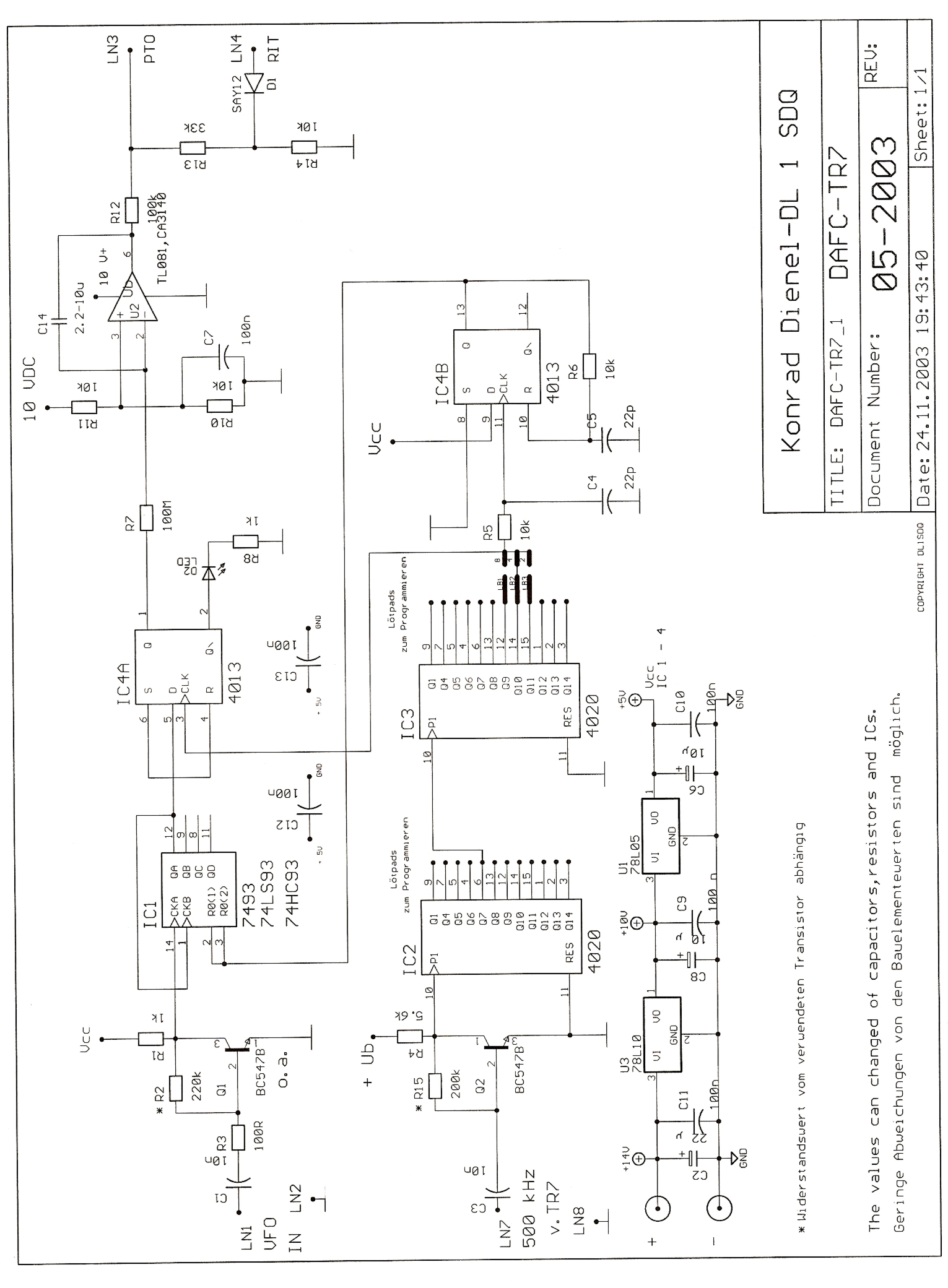
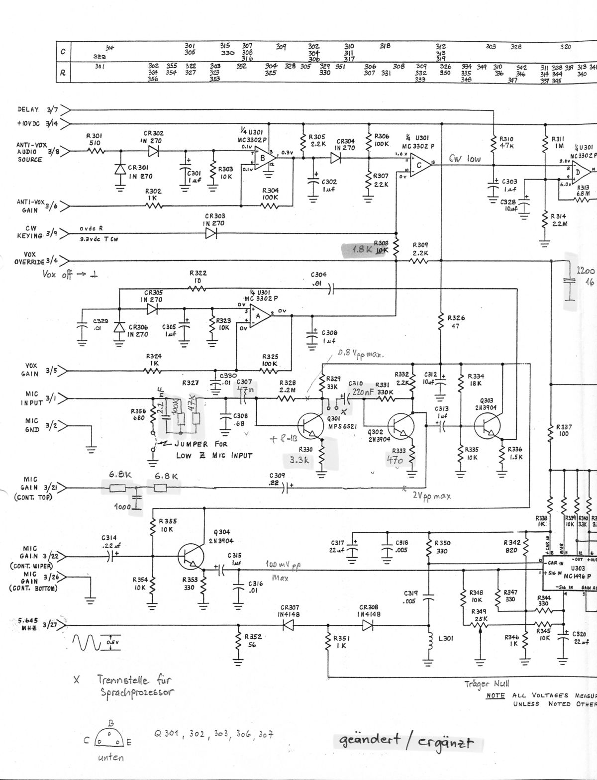
drake-logo-wit.jpg (72207 Byte)

Down Load Gallery

The future of Radio Communications?
Software Defined Radio

Marc van Stralen
Schulstrasse 21 
D-48455  Bad Bentheim
Germany
Last up date: 22-04-14

Bilder zum vergrößern anklicken
Click on pictures to enlarge

E-mail: dk4dds@t-online.de
Phone: +49-(0)5924-997337
Fax: +49(0)5924-997338
Mobile: +49-(0)1577-3326123
Skype: marc.van.stralen
Online Users
Visitors since 08-07-2010:
Besucher ab 08-07-2010:
free counters

CIRCUIT DIAGRAMS / SCHALTBILDER    MANUALS/HANDBÜCHER

Down Load and install Viewer Sprint PCB Lay Out 5.0 to View and Print the PCB Layouts listed on this page
Down Load and install Viewer  sPlan 7.0 to View and Print the Circuit Diagrams listed on this page

You can find these files also at the Site of Abacom www.abacom-online.de

Abacom is a German developer of PCB Layout and   Schematic Editor Software.

Do you need your proto type PCB's ( double and single sided) at very competive prices prices ?

Have a look at the right place!

DK4DDS HAM PROTO PCB POOL SERVICES (UK)


Sie brauchen müster entweder einzel Platinen ?

Einseitig beschichtet entweder Doppleseitig beschichtet für super gunstige Preisen !

DK4DDS HAM PROTO PCB POOL SERVICE (DL)

Down Loads regarding DRAKE TR7

Down Load the de complete renvovation story in English written by DK4DDS in pdf format 2 MB:
Herunterladen Sie die ganze eneuerungs Gesichte von Drake TR7 geschrieben vom DK4DDS im pdf Format 2 MB
Link to the Article: www.wb4hfn.com/DRAKE/DrakeArticles/THE_DRAKE_TR7_RENEWED.pdf

Nederlandstalige afregel procedure X-tal Oscillatoren Drake TR7 !

Nederlandstalige inbouw procedure Lingua Sprachextractor in Drake Tr7

Down Load my Article Regarding the TR7 Published in QST April 2009

High Resolution Drake TR7 Circuitdiagrams A3 Format Could be printed at A4  File Size 6 Megabyte
Schaltbilder TR7 in Höheresolution A3 Format Drücken in A4 ist möglich   Dateigöße 6 Megabyte
Additional Circuit Diagram Pre Driver TR7 PA  File Size 39 kB
Extraschaltbild Vortreiber TR7 Endstufe  Dateigöße 39 kB
User Manual Drake R4C
Operating Manual Signal One Milspec 1030C
Ciruit Digram DAFC FOR DRAKE TR7
Notch Filter for Drake TR7
Circuit Diagram Notch Filter TR7 in PDF
Schaltbild Notchfilter für Drake TR7 in PDF
PCB for TR7 Notch Filter in Sprint Lay Out Format
Component Placement Notch Filter in PDF Format
Bestückungsplan NotchFilter für TR7 in PDF Format
Speech Processor Drake TR7
Schlatbild Geänderte Transmitter Exiter Board TR7
Circuit Diagram Modified Transmitter Exiter Board TR7
Circuit Diagram Speech Processor TR PDF Format
Schaltbild Sprachprozessor TR PDF Format
Component Placement Speech Processor Board
Bestückungsplan   Sprachprozessor
PCB-Speech Processor TR Sprint 5.0 Format
Leiterplatte Sprachprozessor
PIN Diode Attenuator for PA TR7 (see my article in QST April 2009)

Circuit Diagram PIN Diode Attenuator/Schaltbild PIN Dämpfungsregler

Assembly Plan PIN DIODE Attenuator Bestückungsplan PIN Diode Attenuator

PCB Layout PIN Diode Attenuator/Leiterplatte PIN Dämpfungsregler in Sprint 5.0 Format

DC Output Filter for the new TR7 Power Suppply / DC Ausgangs Filter für das neue Netzteils  derTR7
Pre Amplifier(Receiver) for Drake TR7

Circuit Diagram LNA/Schaltbild LNA for Drake TR7

Part List LNA/Stückliste LNA für Drke TR7

PCB Lay Out LNA/ Leiterplatte LNA 1:1

PCB Layout LNA/Leiterplatte 2:1

Assembly Plan LNA/ Bestückungsplan LNA 1:1

Assembly Plan LNA/ Bestückungsplan LNA 2:1

POWER SUPPLY DOWN LOADS


Down Load Links to:

Circuit Diagrams of my Home Brew Linear High Current DC Power Supplies

13.8 V DC 20 Amp with 4 x 2N3055 ua741 ,13.jpg_small.jpg (4964 bytes)
13.8 V DC 20 Amp with 3 x 2N3771 L200 _13.8V _20A _power supply_small.jpg (3779 bytes)
1,25- 125 V DC 10 A TL783 and BDX 67 1,25-125V_ 10_Amp_Power_Suppl _with_TL783C_small.jpg (2665 bytes)


ANTENNA TUNERS & ACCESSORIES


Down Load Links to:
Home Brew Balanced Antenna Tuner with LED Antenna Current Indicators balanced_tuner_open_complete_small.jpg (7495 bytes) balanced _antenna _tuner _jpg_small.jpg (4042 bytes)

Home Brew Balanced Antenna Current Indicator with Moving Coil Instruments

balanced _antenna _current_indicator_jpg_small.jpg (3509 bytes)


MISCELLANEOUS  _  SONSTIGES


Down Load Links to:
Fan Controller Schaltung  / Circuit Diagram fan controller_jpg_small.jpg (2717 bytes)
VOX MODULE FOR TRANSCEIVERS
vox_sdr_one-circuit_diagram.JPG (104134 Byte)
Herunterladen von das Schaltbild in PDF /Down Load Circuit Digram in PDF Format
Herunterladen von VOX Platine in PDF Down Load PCB Layout in PDF Format
Herunterladen von das Schaltbild in S-Plan 7.0 Format / Down Load the Circuit Diagram in S-Plan 7.0 Format
Down Load PCB Layout in Sprint 5.0 Format / Herunterladen von VOX Platine in Sprint 5.0 Format

TEST OSCILLATORS FOR SSB TRANSMITTERS  PRÜFGENERATOR FÜR SSB SENDER


zweiton-ver1.0.jpg (320511 Byte)

Schaltbild Ein-und Zweiton NF Prüfgenerator  Circuitdiagram Single & Dual Tone Test generator

Bestückungsplan Ein-und Zweiton NF Testgenerator   Assemblyplan for the Single & Dual Tone Test Generator
PCB Testgenerator    Leiterplatte Püfgenerator in Sprint Layout Format
Circuitdiagram Single & Dual Tone Prüfgenerator
Schaltbild Ein-und Zweiton NF Testgenerator
Beschreibung Ein-und Zweitongenerator
DIGITAL TEST OSCILLATOR FOR SSB TRANSMITTER DIGITALE PRÜFGENERATOR FÜR SSB SENDER
Schaltbild Ein-und Zweiton NF Prüfgenerator-E-prom Version  Circuitdiagram Digital Single & Dual Tone Test generator
2_tones_generator_e-prom_version_circuit_diagram_jpg.JPG (300821 Byte)
Bestückungsplan Digitale Prüfgenerator Assembly Plan Digital Test Generator
Leiterplatte Digital Test Generator PCB Digital Test Generator (Sprint Format)

Software for E-prom of the digital test generator, will be available on request

Software für die E-prom der Digitale Zweiton NF-Generator machen wir auf Anfrage verfügbahr.

dk4dds@t-online.de

16 Amp 50 V DC Power Supply

Down Load Circuit Diagram Power Supply in pdf Format

Netzteil_500_Watt_Mosfet_PA_jpg.JPG (91789 Byte)

Netzteil 50 V 16 A DC für 500 Mosfet Endstufe

Laden Sie das Schaltbild in pdf Format von das Netztei herunter

Picture of the DC Power Supply buillt in to bottom side  the Mosfet PA

bottom_600watt_pa.jpg (38890 Byte)

Bild von Netzteil eingebaut unten in die 500 Watt Endstufe


Circuit Diagram of the 500 Watt Low Pass Filter Unit for the 500 Watt Mosfet PA

Down Load the Circuit Diagram in PDF Format

dk4dds_500-watt_low_pass_unit_20_08_10_jpg.JPG (126639 Byte)

Schaltblid von das 500 Watt Mosfet Oberwellenfilter für die 500 Mosfet Endstufe

Laden Sie das Schaltbild von 500 Watt Oberwellenfilter herunter

Picture of the Low Pass Filter of the first   Proto Type with out 50 MHz

600watt_low_pass_filters2.jpg (41805 Byte)

Bild von 500 Watt Oberwellenfilter müster ohne 50 Mhz

Automatic Band Decoder Switch for Low Pass Filters of Extrenal Power Amplifiers
With this switch you will be able to switch automatically the low Pass Filters of your external Transisto/7Mosfet PA.
The advantage to manual band switching of this switch is that always the correct LPF will be selected during transmitting.The PIC device will measure the RF output frequency and select very fast the correct low pass filter.
pic-switch-sdr-one-19-05-2011.JPG (20468 Byte)
Down Load the Circuit Diagram in PDF Format
Down Load the Circuit Diagram in S-Plan 7.0 Format

Laden Sie das Schaltbild in PDF Format herunter
Laden Sie das Schaltbid in S Plan 7.0 herunter

rf-detector-switch_may_2011_ver.2.0_SR_one!.JPG (36551 Byte)
Down Load the PCB Layout in PDF Format
Down Load the PCB Layout  Sprint 5.0

Laden Sie das Layout in PDF format herunter
Laden Sie das Layout in Sprint 5.0 herunter

If you need more info please mail me at dk4dds@t-online.de


ESD Safe USB Microscope for inspection pcb´s and assembly/soldering of SMD components

For the assembly AND SOLDERING of Surface Mount Components and inspection of printed circuit boards I have modified a high resolution USB microscope!
First of all I have replaced the stand/feet of the camera by a large ESD safe working area.
Also I have increased the distance between the working area and the microscope using a longer 16 mm rod.
The Microscope distance between the working area is adjustable now from 0 mm and 200 mm..

The original stand of the microscope was replace by a very "thick scrap epoxy materaial plate" of 10 mm and the working area is 370 mm x 240 mm now.
The surface of the epoxy plate has been covered with professional antistatic rubber material.
Which MUST be grounded to earth via 2 meg resistor and connect to a ESD safe wrist strap

This camera is available including software at € 65,95 by www.reichelt.de part no DNT DIGI PROFI select your language at the web site

http://such001.reichelt.de/?SID=10Uc-9mn8AAAIAAHAANms762fb0f26c6b40a6817b6f3d71469c7b;ACTION=446
esd_smd_microscope4-modified1.jpg (55193 Byte) esd_smd_microscope4-modified2.jpg (45916 Byte)
Picture of a hand mounted and hand soldered smd component Larger view of the pcb
camera_pict1.jpg (36771 Byte) camera_pict2.jpg (29583 Byte)
esd_smd_microscope3.jpg (64561 Byte)

final_version_smd_workstation4.jpg (92349 Byte)

final_version_smd_workstation3.jpg (60347 Byte) esd_smd_microscope2.jpg (53409 Byte)


zurück zur Home Page

Back to UK Home Page